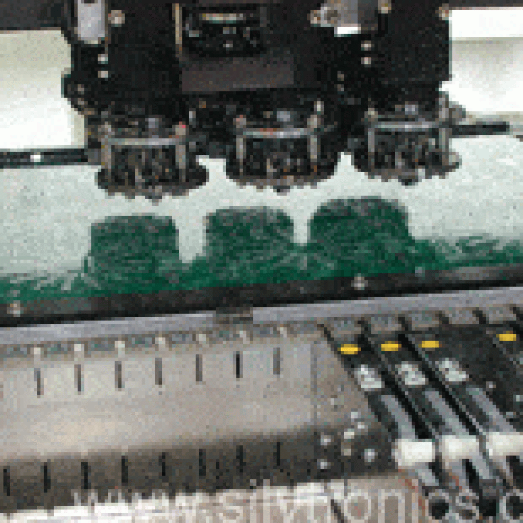
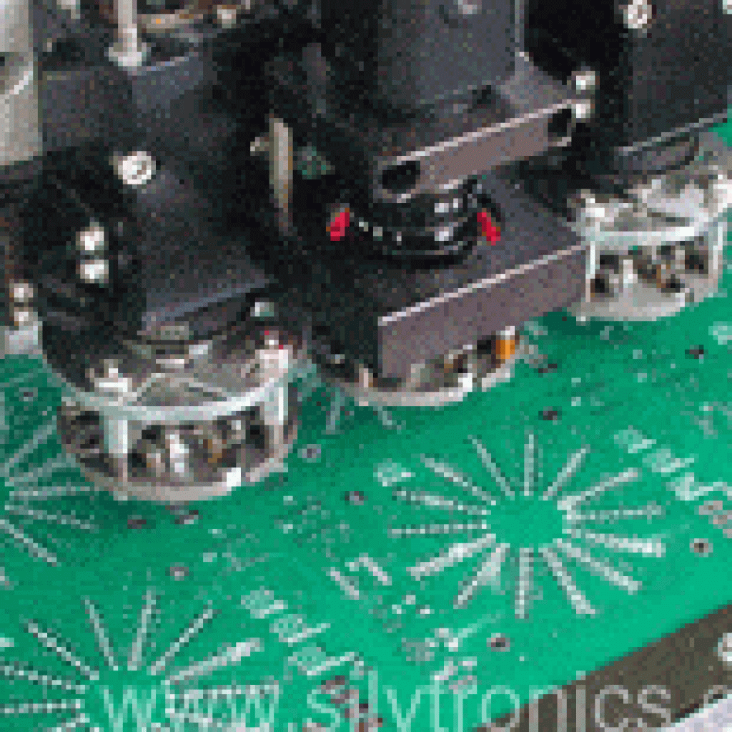
There are two methods for checking PCB defects recognition utilizing image subtraction.
Machine Vision
Machine vision (MV) is the innovation and techniques used to give imaging-based programmed examination and dissection for such requisitions as immediate review, process control, and robot direction in industry.
Machine vision is concerned with the hypothesis behind counterfeit frameworks that concentrate data from pictures and succession of pictures. The picture information can take numerous shapes, for example motion picture arrangements, sees from various Polaroids, or multidimensional information from a medicinal scanner.
Uncovered PCB Deformities
There are some defects that is often discovered on PCB. Conductor breaking causing open connection and conductor shorting causing short connection is described as a serious defects. Pinhole, breakout, over engraving, and under engraving are described as potential deformities. Deadly absconds are those in which the PCB does not go to the target they are intended for, and potential deformities are those trading off the PCB throughout their use. Throughout etching process, the anomalies happening on uncovered PCB could be all in all characterized in two classes: the one is abundance of Copper and the other one is absent copper.
The inadequate etching process leaves unwanted conductive materials and shapes surrenders like short, additional hole, distension, island, and modest space. The intemperate etching makes open, pin hole, scratch (rodent nibble), and meager example. Notwithstanding the imperfections said above, some different deformities might exist on exposed PCB, for instance, missing holes (because of hardware break), scratch (because of taking care of slip-up), and splits.