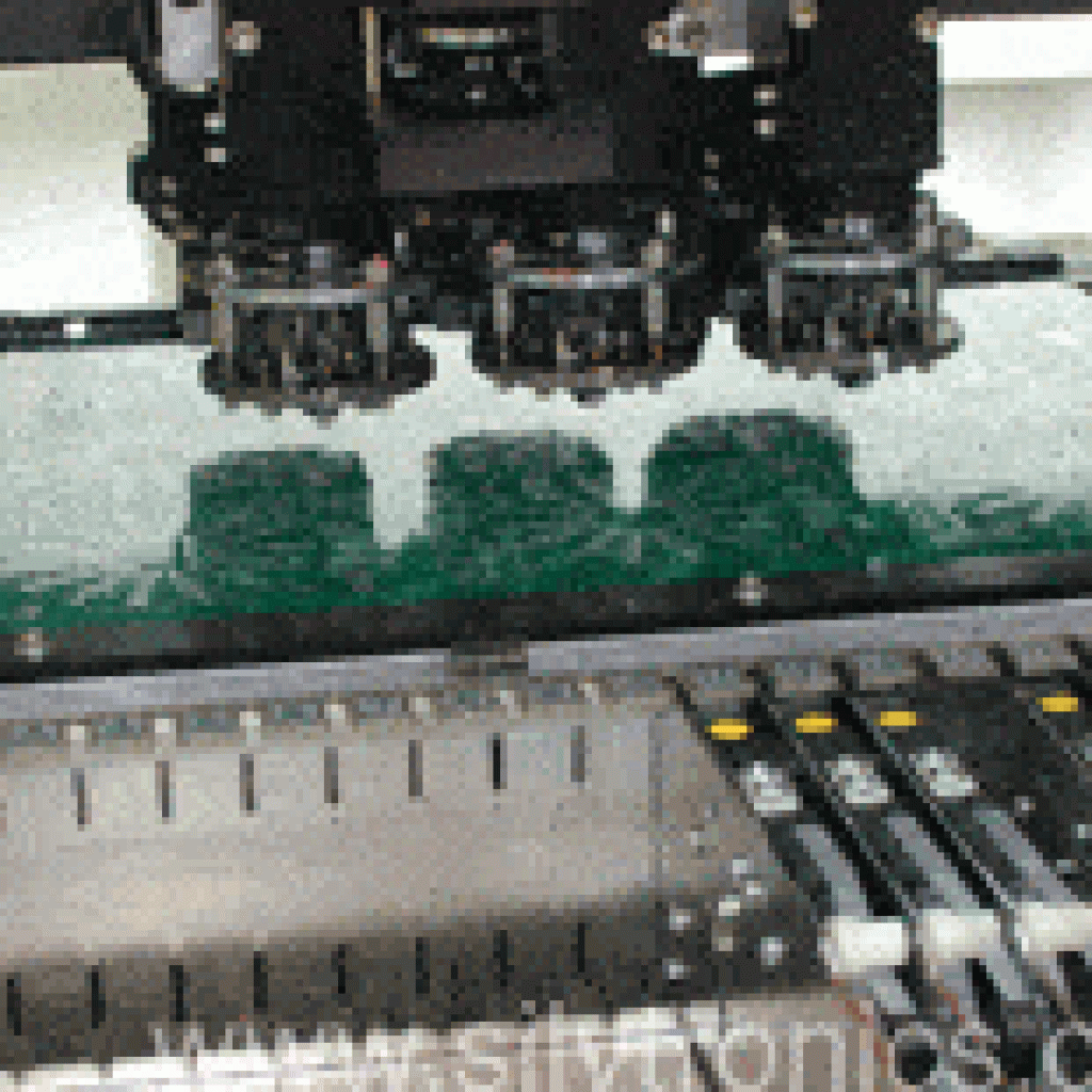
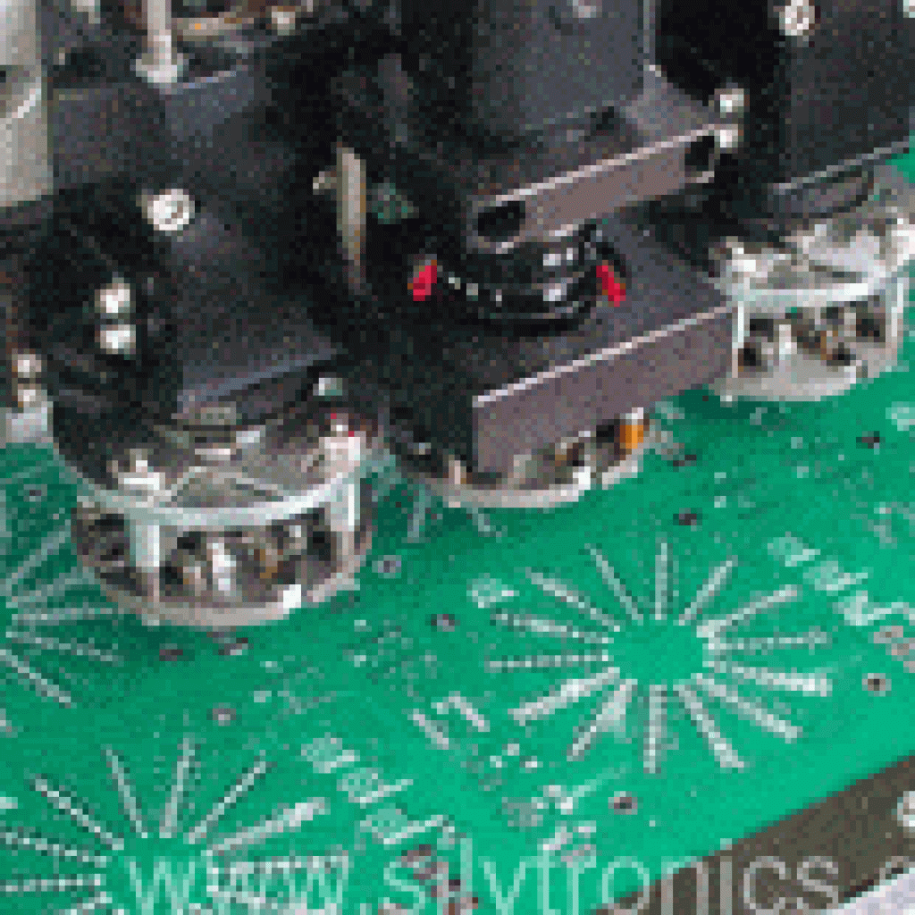
PCB assembly increasingly have bottom termination components, such as QFNs and BGAs. These components are categorized as leadless parts in our PCB Assembly Quote form. These components have hidden solder joints and it is hard to detect defects on the hidden solder joints. Manual visual inspection or automated optical inspection surely cannot detect bad solder joints mainly because the joint is hidden by the component body. Marginal defects involve cases where there is often enough solder present for the connection between the termination on the bottom-side of the component and the board pad that allow the component to pass functional and in-circuit tests. However if the board is exposed to shock or vibration, chances are high that the solder will fracture leading to an open connection. Using 2D x-ray it is very difficult to detect QFN solder joint defects, usually with 2D x-ray a defective solder joint looks almost like a good solder joint.
3D Automated X-ray Inspection analyzes the solder joint profile, takes measurements and compares them against those of a good solder joint. If the joint is defective, it will have different profile measurements from those of a good solder joint.
In a good solder joint, the solder paste wets and the part collapses on the pad creating a wide and thin solder joint. A bad solder joint will have no wetting, leading to an open joint. The characteristics of an open joint include a higher solder center thickness measurement, a narrower center width, and a smaller slope of the outer edges of the joint. 3D AXI is capable of taking measurements of these various characteristics of good QFN solder joints and set them as standard values for use in the testing of components on subsequent boards.